


说明
Darkfield inspection配置
无配置OEM 型号描述
AIT UV™ is a high-throughput, high-sensitivity wafer inspection product that uses Dual AOD technology to increase scan rate, UV laser illumination for increased sensitivity, and advanced detection algorithms for improved defect capture. It also features real-time Adaptive Mode™ technology, three-channel double-darkfield optics, MultiSpot™ illumination, and Inline Automatic Defect Classification (iADC) for faster results. It is part of KLA-Tencor’s AIT family of inspection systems and is designed for 300-mm inspection and excursion monitoring at 100-nm design rules and below.文件
无文件

类似上架物品
查看全部
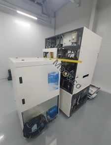
KLA
AIT UV
类别
Defect Inspection
上次验证: 60 多天前


物品主要详细信息
状况:
Used
运行状况:
未知
产品编号:
112936
晶圆尺寸:
12"/300mm
年份:
2005
Logistics Support
Available
Transaction Insured by Moov
Available
Refurbishment Services
Available
说明
Darkfield inspection配置
无配置OEM 型号描述
AIT UV™ is a high-throughput, high-sensitivity wafer inspection product that uses Dual AOD technology to increase scan rate, UV laser illumination for increased sensitivity, and advanced detection algorithms for improved defect capture. It also features real-time Adaptive Mode™ technology, three-channel double-darkfield optics, MultiSpot™ illumination, and Inline Automatic Defect Classification (iADC) for faster results. It is part of KLA-Tencor’s AIT family of inspection systems and is designed for 300-mm inspection and excursion monitoring at 100-nm design rules and below.文件
无文件