


说明
无说明配置
无配置OEM 型号描述
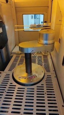
The Surfscan SP2 is an unpatterned wafer surface inspection tool that uses UV laser technology, darkfield optics, and advanced algorithms to detect defects as small as 30nm. It provides high sensitivity detection on engineered substrates and has a significant throughput increase over the prior-generation tool. It offers a single tool solution for three technology nodes and has comprehensive wafer surface inspection capabilities. It also enables faster root-cause analysis with improved coordinate accuracy and real-time defect classification capability.文件
无文件

类别
Defect Inspection
上次验证: 60 多天前
物品主要详细信息
状况:
Used
运行状况:
Deinstalled
产品编号:
128959
晶圆尺寸:
12"/300mm
年份:
未知
Logistics Support
Available
Transaction Insured by Moov
Available
Refurbishment Services
Available
类似上架物品
查看全部


KLA
SURFSCAN SP2
类别
Defect Inspection
上次验证: 60 多天前


物品主要详细信息
状况:
Used
运行状况:
Deinstalled
产品编号:
128959
晶圆尺寸:
12"/300mm
年份:
未知
Logistics Support
Available
Transaction Insured by Moov
Available
Refurbishment Services
Available
说明
无说明配置
无配置OEM 型号描述
The Surfscan SP2 is an unpatterned wafer surface inspection tool that uses UV laser technology, darkfield optics, and advanced algorithms to detect defects as small as 30nm. It provides high sensitivity detection on engineered substrates and has a significant throughput increase over the prior-generation tool. It offers a single tool solution for three technology nodes and has comprehensive wafer surface inspection capabilities. It also enables faster root-cause analysis with improved coordinate accuracy and real-time defect classification capability.文件
无文件