



说明
Etch / ashing system配置
(Qty 3) Standard chambersOEM 型号描述
The AMAT CENTURA eMAX ETCH is an advanced dielectric etch system designed for fabricating semiconductor chip structures with feature sizes as small as 0.13 microns and beyond. It optimizes etching, photoresist strip, and barrier removal in a single chamber, reducing costs and cycle times. The system supports various applications, including etch, epitaxy, CVD, RTP, and plasma nitration. Its integration with existing Centura platforms allows for enhanced flexibility and adaptation to different process requirements. Introduced in June 2000, the eMAX ETCH specializes in etching a wide range of dielectric films, crucial for producing high-precision and reliable semiconductor devices in the contact and interconnect regions of chips. The Dielectric Etch eMax Centura was introduced in June 2000 as an extension of Applied's MxP+ and Super e dielectric process chamber designs. The Applied Centura eMax system etches a broad range of dielectric films in the contact and interconnect regions of the chip.文件
无文件

类别
Dry / Plasma Etch
上次验证: 13 天前
物品主要详细信息
状况:
Used
运行状况:
未知
产品编号:
152688
晶圆尺寸:
12"/300mm
年份:
2004
Logistics Support
Available
Transaction Insured by Moov
Available
Refurbishment Services
Available
类似上架物品
查看全部
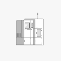
APPLIED MATERIALS (AMAT)
CENTURA eMAX ETCH
类别
Dry / Plasma Etch
上次验证: 13 天前


物品主要详细信息
状况:
Used
运行状况:
未知
产品编号:
152688
晶圆尺寸:
12"/300mm
年份:
2004
Logistics Support
Available
Transaction Insured by Moov
Available
Refurbishment Services
Available
说明
Etch / ashing system配置
(Qty 3) Standard chambersOEM 型号描述
The AMAT CENTURA eMAX ETCH is an advanced dielectric etch system designed for fabricating semiconductor chip structures with feature sizes as small as 0.13 microns and beyond. It optimizes etching, photoresist strip, and barrier removal in a single chamber, reducing costs and cycle times. The system supports various applications, including etch, epitaxy, CVD, RTP, and plasma nitration. Its integration with existing Centura platforms allows for enhanced flexibility and adaptation to different process requirements. Introduced in June 2000, the eMAX ETCH specializes in etching a wide range of dielectric films, crucial for producing high-precision and reliable semiconductor devices in the contact and interconnect regions of chips. The Dielectric Etch eMax Centura was introduced in June 2000 as an extension of Applied's MxP+ and Super e dielectric process chamber designs. The Applied Centura eMax system etches a broad range of dielectric films in the contact and interconnect regions of the chip.文件
无文件