


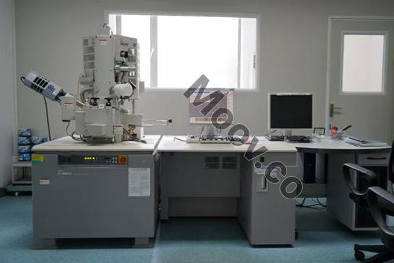
说明
Scanning Electron Microscope (SEM)配置
Electron source: Cold-cathode field emission Accelerating voltage: 0.5-30 kV, in 0.1 kV steps Magnification: 20×-800,000× Beam current range: 1 pA-2 nA Standard detectors: SE / BE, E×B combined detector Imaging modes: Secondary-electron morphology / Backscattered-electron atomic-number contrast Beam deceleration: Yes Secondary-electron resolution: 1.0 nm at 15 kV, 4 mm working distance 2.0 nm at 1 kV, 1.5 mm working distance, normal mode 1.4 nm at 1 kV, 1.5 mm working distance, beam-deceleration mode Specimen stage - Five-axis motorized: X travel: 0-50 mm Y travel: 0-50 mm Z travel: 1.5-30 mm Tilt: -5° to +70° Rotation: Continuous 360° Maximum specimen diameter: 100 mm Vacuum: Specimen chamber: 7 × 10⁻⁴ Pa Electron-gun chamber: 1 × 10⁻⁷ PaOEM 型号描述
The S-4800 is an advanced Field Emission Scanning Electron Microscope (FE-SEM) that builds upon the proven performance of its predecessors, the S-4700 and S-5200. With beam deceleration technology, it achieves an impressive resolution of 1.4 nm at 1 kV and 1.0 nm at 15 kV. The microscope features a semi-in-lens detector design, allowing for the examination of large samples without compromising ultra-high resolution at low accelerating voltages. The innovative objective lens design incorporates Hitachi's Super ExB filter technology, which effectively separates pure secondary electrons (SE), compositional SE, and backscattered electron (BSE) signals. With a specimen diameter of 200 mm and a 5-axis motorized eucentric stage, it offers exceptional sample accommodation and positioning capabilities. The S-4800 is compatible with optional accessories such as Energy Dispersive X-ray Spectrometer (EDX) and Electron Backscatterted Diffraction Pattern (EBDP) systems, making it suitable for a range of ultra-high resolution applications in fields like semiconductor research, materials studies, and nanotechnology.文件
无文件

类似上架物品
查看全部




HITACHI
S-4800
类别
SEM / FIB
上次验证: 昨天


物品主要详细信息
状况:
Used
运行状况:
未知
产品编号:
154501
晶圆尺寸:
未知
年份:
未知
Logistics Support
Available
Transaction Insured by Moov
Available
Refurbishment Services
Available
说明
Scanning Electron Microscope (SEM)配置
Electron source: Cold-cathode field emission Accelerating voltage: 0.5-30 kV, in 0.1 kV steps Magnification: 20×-800,000× Beam current range: 1 pA-2 nA Standard detectors: SE / BE, E×B combined detector Imaging modes: Secondary-electron morphology / Backscattered-electron atomic-number contrast Beam deceleration: Yes Secondary-electron resolution: 1.0 nm at 15 kV, 4 mm working distance 2.0 nm at 1 kV, 1.5 mm working distance, normal mode 1.4 nm at 1 kV, 1.5 mm working distance, beam-deceleration mode Specimen stage - Five-axis motorized: X travel: 0-50 mm Y travel: 0-50 mm Z travel: 1.5-30 mm Tilt: -5° to +70° Rotation: Continuous 360° Maximum specimen diameter: 100 mm Vacuum: Specimen chamber: 7 × 10⁻⁴ Pa Electron-gun chamber: 1 × 10⁻⁷ PaOEM 型号描述
The S-4800 is an advanced Field Emission Scanning Electron Microscope (FE-SEM) that builds upon the proven performance of its predecessors, the S-4700 and S-5200. With beam deceleration technology, it achieves an impressive resolution of 1.4 nm at 1 kV and 1.0 nm at 15 kV. The microscope features a semi-in-lens detector design, allowing for the examination of large samples without compromising ultra-high resolution at low accelerating voltages. The innovative objective lens design incorporates Hitachi's Super ExB filter technology, which effectively separates pure secondary electrons (SE), compositional SE, and backscattered electron (BSE) signals. With a specimen diameter of 200 mm and a 5-axis motorized eucentric stage, it offers exceptional sample accommodation and positioning capabilities. The S-4800 is compatible with optional accessories such as Energy Dispersive X-ray Spectrometer (EDX) and Electron Backscatterted Diffraction Pattern (EBDP) systems, making it suitable for a range of ultra-high resolution applications in fields like semiconductor research, materials studies, and nanotechnology.文件
无文件