


说明
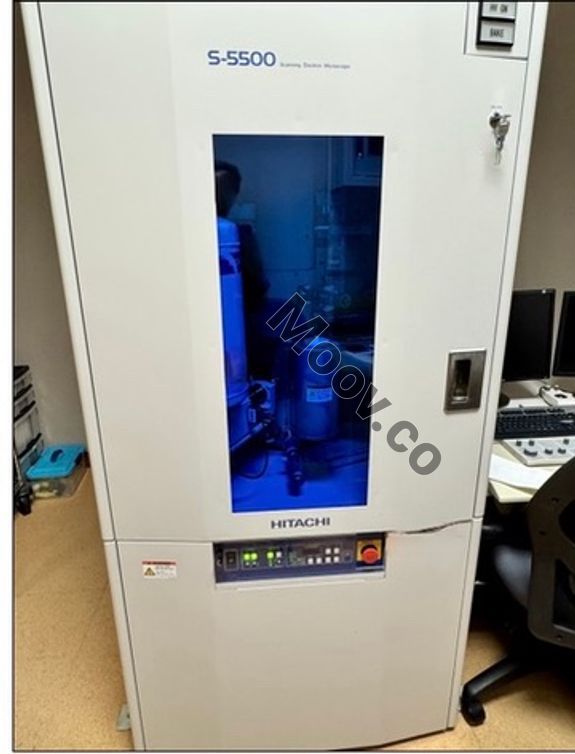
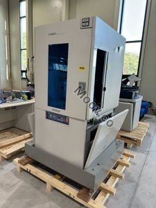
Scanning Electron Microscope in‑lens cold field‑emission SEM designed for ultra‑high‑resolution imaging and advanced STEM analysis Good vacuum, the electron beam aligns properly, and the system is able to generate stable imaging. Core electron‑optical functions are operational. Known Issues: The sample holder is currently stuck in the main chamber, preventing sample exchange. The system powers on and images, but the stage cannot be reloaded until the holder is released. This issue may require mechanical intervention, vacuum cycling, or vendor service配置
Cold field‑emission electron gun — high brightness and stable probe performance Accelerating voltage range: 0.5–30 kV In‑lens objective design — optimized for sub‑nanometer resolution SE/BSE mixed‑signal detector — blended contrast for surface and material imaging BF/DF Duo‑STEM detector — bright‑field and dark‑field STEM modes Magnification range: ×60 to ×2,000,000 Dry vacuum system — oil‑free, stable long‑term operation EDS compatible — supports standard SDD detectors Specimen size capacity: Plan‑view: 5.0 × 9.5 × 3.8 mm Cross‑section: 2.0 × 6.5 × 5.0 mmOEM 型号描述
The S-5500, Immersion Lens system which generates the highest resolution images in the world(*1)(0.4nm at 30kV. The S-5500 have improved performance over that of its predecessor, the S-5200. [Main features of S-5500] (1) The world’s highest resolution, 0.4 nm at 30 kV, achieved by the use of a new electron optics system (as of October 2004). (2) New BF (bright field)/ DF (dark field) Duo STEM (scanning transmission electron microscopy) detector allows simultaneous display of BF and DF STEM images. In DF STEM mode, this detector is capable of providing images with variable detection angles. This new detection system greatly extends the usage of low accelerating voltage STEM at 30 kV.文件
无文件

类似上架物品
查看全部





HITACHI
S-5500
类别
SEM / FIB
上次验证: 6 天前


物品主要详细信息
状况:
Used
运行状况:
未知
产品编号:
149108
晶圆尺寸:
未知
年份:
未知
Logistics Support
Available
Transaction Insured by Moov
Available
Refurbishment Services
Available
说明
Scanning Electron Microscope in‑lens cold field‑emission SEM designed for ultra‑high‑resolution imaging and advanced STEM analysis Good vacuum, the electron beam aligns properly, and the system is able to generate stable imaging. Core electron‑optical functions are operational. Known Issues: The sample holder is currently stuck in the main chamber, preventing sample exchange. The system powers on and images, but the stage cannot be reloaded until the holder is released. This issue may require mechanical intervention, vacuum cycling, or vendor service配置
Cold field‑emission electron gun — high brightness and stable probe performance Accelerating voltage range: 0.5–30 kV In‑lens objective design — optimized for sub‑nanometer resolution SE/BSE mixed‑signal detector — blended contrast for surface and material imaging BF/DF Duo‑STEM detector — bright‑field and dark‑field STEM modes Magnification range: ×60 to ×2,000,000 Dry vacuum system — oil‑free, stable long‑term operation EDS compatible — supports standard SDD detectors Specimen size capacity: Plan‑view: 5.0 × 9.5 × 3.8 mm Cross‑section: 2.0 × 6.5 × 5.0 mmOEM 型号描述
The S-5500, Immersion Lens system which generates the highest resolution images in the world(*1)(0.4nm at 30kV. The S-5500 have improved performance over that of its predecessor, the S-5200. [Main features of S-5500] (1) The world’s highest resolution, 0.4 nm at 30 kV, achieved by the use of a new electron optics system (as of October 2004). (2) New BF (bright field)/ DF (dark field) Duo STEM (scanning transmission electron microscopy) detector allows simultaneous display of BF and DF STEM images. In DF STEM mode, this detector is capable of providing images with variable detection angles. This new detection system greatly extends the usage of low accelerating voltage STEM at 30 kV.文件
无文件