


说明
FPA-5000ES2+ (KrF)配置
无配置OEM 型号描述
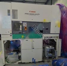
The FPA-5000ES2+ is a high-throughput 248-nanometer scanner for 0.15-micron ICs, introduced by Canon U.S.A. Inc.'s Semiconductor Equipment Division. It uses a 2-kilohertz, krypton-fluoride (KrF) excimer laser to expose 125 eight-inch wafers an hour and is aimed at a growing need for highly productive scanners with both 200- and 300-mm wafer capability. It has been designed to handle both 0.18- and 0.15-micron design rules, and allows field conversion from 200-mm to 300-mm wafer format within a day. It offers a 25% increase in throughput compared with its predecessor, the FPA-5000ES2.文件
无文件

类别
Steppers & Scanners
上次验证: 60 多天前
物品主要详细信息
状况:
Used
运行状况:
未知
产品编号:
109624
晶圆尺寸:
8"/200mm
年份:
未知
Logistics Support
Available
Transaction Insured by Moov
Available
Refurbishment Services
Available


CANON
FPA-5000ES2+
类别
Steppers & Scanners
上次验证: 60 多天前


物品主要详细信息
状况:
Used
运行状况:
未知
产品编号:
109624
晶圆尺寸:
8"/200mm
年份:
未知
Logistics Support
Available
Transaction Insured by Moov
Available
Refurbishment Services
Available
说明
FPA-5000ES2+ (KrF)配置
无配置OEM 型号描述
The FPA-5000ES2+ is a high-throughput 248-nanometer scanner for 0.15-micron ICs, introduced by Canon U.S.A. Inc.'s Semiconductor Equipment Division. It uses a 2-kilohertz, krypton-fluoride (KrF) excimer laser to expose 125 eight-inch wafers an hour and is aimed at a growing need for highly productive scanners with both 200- and 300-mm wafer capability. It has been designed to handle both 0.18- and 0.15-micron design rules, and allows field conversion from 200-mm to 300-mm wafer format within a day. It offers a 25% increase in throughput compared with its predecessor, the FPA-5000ES2.文件
无文件