


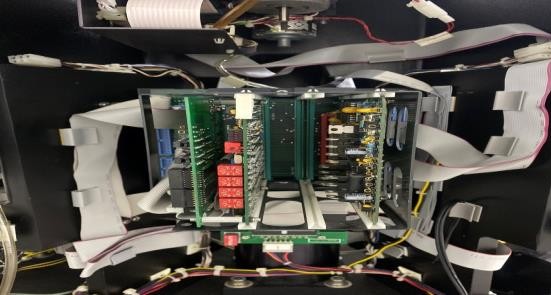
说明
Supported SEMI/JEIDA Geometries Wafer diameters supported: 125mm, 150mm, 200mm (polished or patterned) Wafer thickness: 400 um to 800 um Notches, Flats(primary/Secondary): Up to four(4) per SEMI and JEIDA standards Edge Exclusion: To 3 mm from edge (2mm optional) Measurement and sorting Thickness Center point, Five point, Full wafer scan Shape: Bow, Warp, using 3-point & Best-fit references Global Flatness: SEMI GBI ,TIR, FPD, FPD%, 5-point TTV Site Flatness: All SEMI M1 Standards with 8 – 30mm sit size and variable site offsets Data Density and Throughput Number of thickness/shape data points: Up to 17300 points Throughput using optional handler: 30 – 59+ wafer/hour ( depends on wafer size, measurement pattern and mode System Consist of: System Consist of: Cassette input stations*2 Cassette output stations*3 Pal station *1 E-plus station *1 Rest station*1 ASC Controller*1 ADE single robot station*1 ADE robot controller*1 Main DC power*1 Delivery time: 4 months Option Choice upgrade tools Controller function open (edge 2mm) Signal effector arm Robot upgrade to Duel effector arm robot ASC Controller upgrade to ASC 2000 UPS(C-10000F) Non-contact P/N Type tester: For wafer resistivity from 0.1 to 200ohm-cm配置
无配置OEM 型号描述
UltraScan Wafer Metrology System The 9600 and 9650 systems, introduced in 1994 and based on the more advanced E-Plus station, measure thickness down to an accuracy of 0.25 microns.文件


类别
Thin Film / Film Thickness
上次验证: 30 多天前
物品主要详细信息
状况:
Refurbished
运行状况:
未知
产品编号:
150818
晶圆尺寸:
5"/125mm, 6"/150mm, 8"/200mm
年份:
未知
Logistics Support
Available
Transaction Insured by Moov
Available
Refurbishment Services
Available

KLA / ADE
ULTRASCAN 9600
类别
Thin Film / Film Thickness
上次验证: 30 多天前


物品主要详细信息
状况:
Refurbished
运行状况:
未知
产品编号:
150818
晶圆尺寸:
5"/125mm, 6"/150mm, 8"/200mm
年份:
未知
Logistics Support
Available
Transaction Insured by Moov
Available
Refurbishment Services
Available