


说明
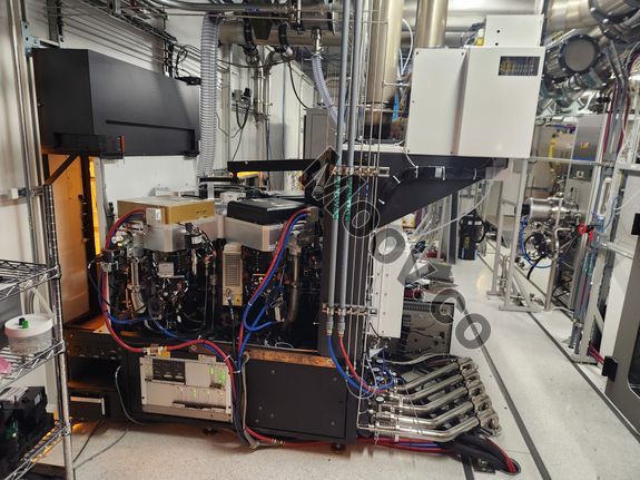
Plasma enhanced chemical vapor deposition (PECVD) system配置
(Qty 2) PECVD DxL chambers (Qty 1) PECVD DxL TEOS chamber (Qty 1) RIE chamber Deposition materials: Amorphous silicon / silicon oxide / silicon nitride Smaller substrates supported using a carrier Vacuum system: (Qty 4) Edwards IQDP40 chamber pumps with QMB250 boosters Edwards IQDP40 load lock pump Gas delivery: MFCs and plumbing for Ar / C2F6 / H2 / He / N2 / N2O / NH3 / O2 / SiH4 Additional installed gas lines and MFCs: B2H6-H2 / BF3 / CH4 / GeH4 / PH3OEM 型号描述
The Applied Materials Precision 5000 CVD is a single system solution for depositing high-quality, low-temperature dielectric materials on semiconductor devices. It incorporates multi-step processes to provide enabling technology for void-free intermetal dielectric deposition with profile control. The system’s process flexibility over a wide range of applications reduces the number and types of machines required for CVD. This makes it an efficient and cost-effective solution for semiconductor manufacturing.文件
无文件

类别
CVD
上次验证: 7 天前
物品主要详细信息
状况:
Used
运行状况:
未知
产品编号:
156354
晶圆尺寸:
8"/200mm
年份:
未知
Logistics Support
Available
Transaction Insured by Moov
Available
Refurbishment Services
Available
类似上架物品
查看全部


APPLIED MATERIALS (AMAT)
P5000 CVD
类别
CVD
上次验证: 7 天前


物品主要详细信息
状况:
Used
运行状况:
未知
产品编号:
156354
晶圆尺寸:
8"/200mm
年份:
未知
Logistics Support
Available
Transaction Insured by Moov
Available
Refurbishment Services
Available
说明
Plasma enhanced chemical vapor deposition (PECVD) system配置
(Qty 2) PECVD DxL chambers (Qty 1) PECVD DxL TEOS chamber (Qty 1) RIE chamber Deposition materials: Amorphous silicon / silicon oxide / silicon nitride Smaller substrates supported using a carrier Vacuum system: (Qty 4) Edwards IQDP40 chamber pumps with QMB250 boosters Edwards IQDP40 load lock pump Gas delivery: MFCs and plumbing for Ar / C2F6 / H2 / He / N2 / N2O / NH3 / O2 / SiH4 Additional installed gas lines and MFCs: B2H6-H2 / BF3 / CH4 / GeH4 / PH3OEM 型号描述
The Applied Materials Precision 5000 CVD is a single system solution for depositing high-quality, low-temperature dielectric materials on semiconductor devices. It incorporates multi-step processes to provide enabling technology for void-free intermetal dielectric deposition with profile control. The system’s process flexibility over a wide range of applications reduces the number and types of machines required for CVD. This makes it an efficient and cost-effective solution for semiconductor manufacturing.文件
无文件