


说明
无说明配置
0.050 um Defect Sensitivity on Polished Bare Silicon Enhanced Rough Film Sensitivity Already upgraded with ENH SS laser Defect Map and Histogram with Zoom RTDC (Real Time Defect Classification) Map to Map Operator Interface Blower UnitOEM 型号描述
The Surfscan SP1DLS is an unpatterned wafer inspection system that detects defects down to 50nm and provides complete defectivity and haze information in a single scan. It uses dual-laser illumination and has an optional Backside Inspection Module. It supports 200mm and 300mm wafer sizes and meets 300mm factory automation requirements.文件
无文件

类似上架物品
查看全部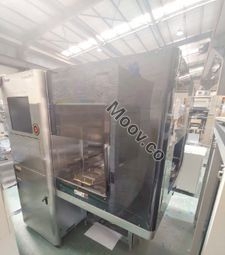


KLA
SP1 DLS
类别
Defect Inspection
上次验证: 60 多天前


物品主要详细信息
状况:
Used
运行状况:
未知
产品编号:
123843
晶圆尺寸:
未知
年份:
2004
Logistics Support
Available
Transaction Insured by Moov
Available
Refurbishment Services
Available
说明
无说明配置
0.050 um Defect Sensitivity on Polished Bare Silicon Enhanced Rough Film Sensitivity Already upgraded with ENH SS laser Defect Map and Histogram with Zoom RTDC (Real Time Defect Classification) Map to Map Operator Interface Blower UnitOEM 型号描述
The Surfscan SP1DLS is an unpatterned wafer inspection system that detects defects down to 50nm and provides complete defectivity and haze information in a single scan. It uses dual-laser illumination and has an optional Backside Inspection Module. It supports 200mm and 300mm wafer sizes and meets 300mm factory automation requirements.文件
无文件