


说明
(E4 Frame) ETCHER配置
无配置OEM 型号描述
The 2300 Versys Kiyo45 is a Reactive Ion Etch (RIE) system from Lam Research, part of the Kiyo Product Family. It is used to shape the electrically active materials of a semiconductor device with high precision and consistency. The Kiyo product family is known for its high-performance capabilities and productivity. The Versys Kiyo45 is used for various applications, including shallow trench isolation, source/drain engineering, high-k/metal gate, FinFET and tri-gate, and multi-patterning. It enables processing at sub-65 nm technology nodes.文件
无文件

类别
Dry / Plasma Etch
上次验证: 60 多天前
物品主要详细信息
状况:
Used
运行状况:
未知
产品编号:
127499
晶圆尺寸:
未知
年份:
2011
Logistics Support
Available
Transaction Insured by Moov
Available
Refurbishment Services
Available
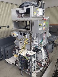

LAM RESEARCH CORPORATION
2300 VERSYS KIYO45
类别
Dry / Plasma Etch
上次验证: 60 多天前


物品主要详细信息
状况:
Used
运行状况:
未知
产品编号:
127499
晶圆尺寸:
未知
年份:
2011
Logistics Support
Available
Transaction Insured by Moov
Available
Refurbishment Services
Available
说明
(E4 Frame) ETCHER配置
无配置OEM 型号描述
The 2300 Versys Kiyo45 is a Reactive Ion Etch (RIE) system from Lam Research, part of the Kiyo Product Family. It is used to shape the electrically active materials of a semiconductor device with high precision and consistency. The Kiyo product family is known for its high-performance capabilities and productivity. The Versys Kiyo45 is used for various applications, including shallow trench isolation, source/drain engineering, high-k/metal gate, FinFET and tri-gate, and multi-patterning. It enables processing at sub-65 nm technology nodes.文件
无文件