


说明
无说明配置
无配置OEM 型号描述
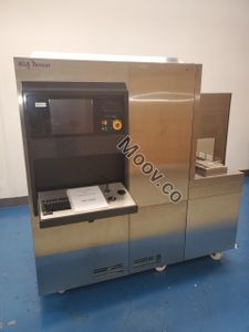
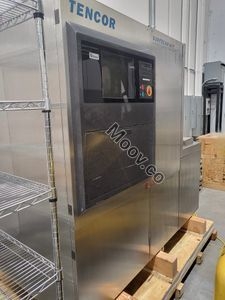
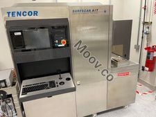
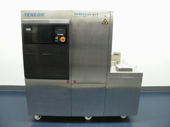
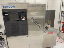
The AIT In-line Defect Inspection System is a high-throughput system that uses proprietary double-darkfield (DDF) laser scanning technology to detect defects, microscratches, and particulate contamination on wafers. It can inspect up to 30 wafers per hour at maximum sensitivity and has a low cost-per-inspection, making it economically feasible to perform in-line process monitoring at more process levels. The system achieves exceptional defect sensitivity through innovations such as a reduced laser spot size and a unique double-darkfield laser scattering design.文件
无文件

类似上架物品
查看全部


KLA
AIT I
类别
Defect Inspection
上次验证: 60 多天前


物品主要详细信息
状况:
Used
运行状况:
未知
产品编号:
126907
晶圆尺寸:
未知
年份:
1998
Logistics Support
Available
Transaction Insured by Moov
Available
Refurbishment Services
Available
说明
无说明配置
无配置OEM 型号描述
The AIT In-line Defect Inspection System is a high-throughput system that uses proprietary double-darkfield (DDF) laser scanning technology to detect defects, microscratches, and particulate contamination on wafers. It can inspect up to 30 wafers per hour at maximum sensitivity and has a low cost-per-inspection, making it economically feasible to perform in-line process monitoring at more process levels. The system achieves exceptional defect sensitivity through innovations such as a reduced laser spot size and a unique double-darkfield laser scattering design.文件
无文件