


说明
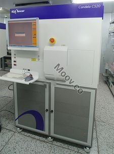
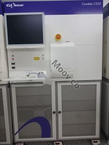
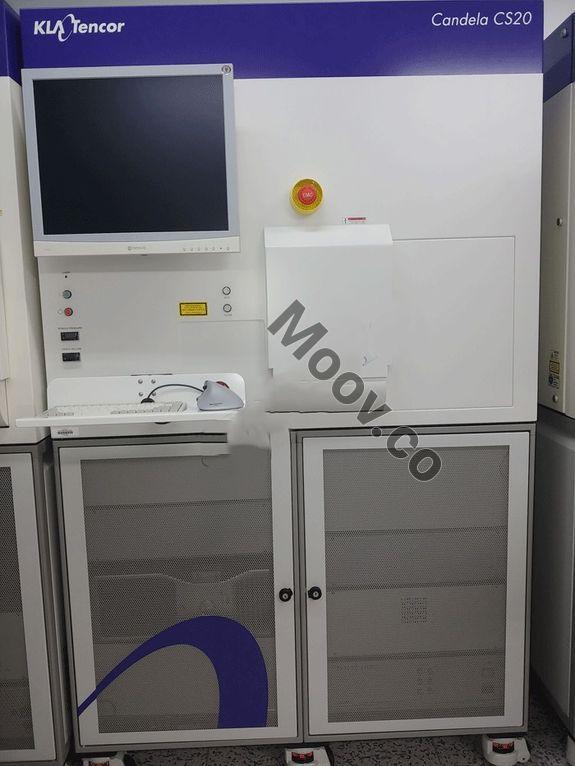
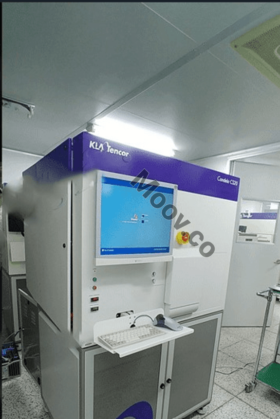
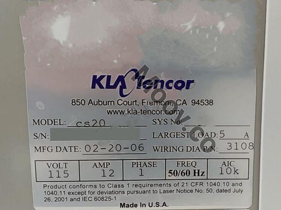
KLA-Tencor Candela CS20 Optical Defect Inspection配置
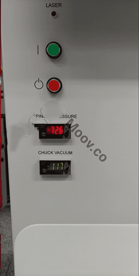
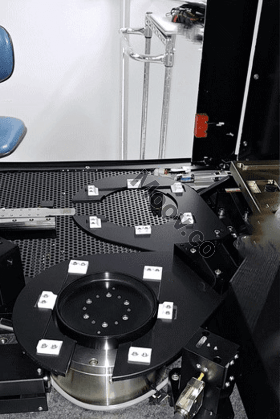
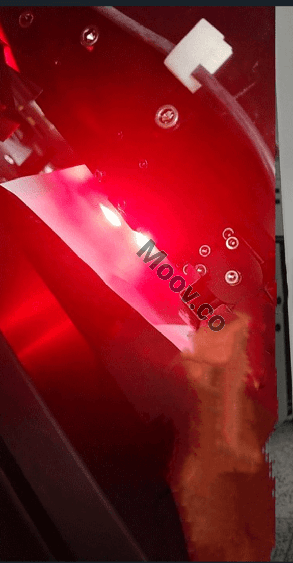
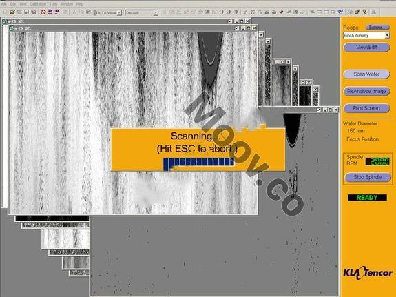
Wafer Size : 2 ~8 inch Illumination Source : 8mW laser, 635 nm wavelength Operator Interface : Trackball and keyboard standard Substrate Thickness : 350 μm ~ 1,100 μm Substrate Material : Any clear or opaque polished surface [ Performance ] Defect Sensitivity 0.08 μm diameter PSL sphere equivalent > 95% capture rate(PSL on bare Si) Other Defects and Applications : Particles, scratches, stains, pits, and bumps. Sensitivity: Minimum detectable size for automatic defect classification: - Scratches: 100 μm long, 0.1 μm wide, 50 Å; deep. - Pits: 20 μm diameter, 50 Å; deep - Stains: 20 μm diameter, 10 Å; thick [ Application ] - Opaque substrates - EPI Layers - Transparent film coatings (SiC, GaN, SapphireOEM 型号描述
The Candela CS20 system measures surface reflectivity and topography for automatic defect detection and classification. It uses scatterometry, ellipsometry, reflectometry, and topographical analysis to inspect wafer surfaces for defects and film thickness uniformity. It is designed for inspection of transparent materials such as sapphire and GaN and can detect a wide variety of defects. It is suitable for use in the production of High Brightness Light Emitting Diodes (HBLEDs), High-Power RF Devices, and Coated Glass (CMOS imagers, LCoS chips, etc.).文件
无文件

类别
Defect Inspection
上次验证: 60 多天前
物品主要详细信息
状况:
Used
运行状况:
未知
产品编号:
101990
晶圆尺寸:
6"/150mm
年份:
2006
Logistics Support
Available
Transaction Insured by Moov
Available
Refurbishment Services
Available
类似上架物品
查看全部


KLA
CANDELA CS20
类别
Defect Inspection
上次验证: 60 多天前

物品主要详细信息
状况:
Used
运行状况:
未知
产品编号:
101990
晶圆尺寸:
6"/150mm
年份:
2006
Logistics Support
Available
Transaction Insured by Moov
Available
Refurbishment Services
Available
说明
KLA-Tencor Candela CS20 Optical Defect Inspection配置
Wafer Size : 2 ~8 inch Illumination Source : 8mW laser, 635 nm wavelength Operator Interface : Trackball and keyboard standard Substrate Thickness : 350 μm ~ 1,100 μm Substrate Material : Any clear or opaque polished surface [ Performance ] Defect Sensitivity 0.08 μm diameter PSL sphere equivalent > 95% capture rate(PSL on bare Si) Other Defects and Applications : Particles, scratches, stains, pits, and bumps. Sensitivity: Minimum detectable size for automatic defect classification: - Scratches: 100 μm long, 0.1 μm wide, 50 Å; deep. - Pits: 20 μm diameter, 50 Å; deep - Stains: 20 μm diameter, 10 Å; thick [ Application ] - Opaque substrates - EPI Layers - Transparent film coatings (SiC, GaN, SapphireOEM 型号描述
The Candela CS20 system measures surface reflectivity and topography for automatic defect detection and classification. It uses scatterometry, ellipsometry, reflectometry, and topographical analysis to inspect wafer surfaces for defects and film thickness uniformity. It is designed for inspection of transparent materials such as sapphire and GaN and can detect a wide variety of defects. It is suitable for use in the production of High Brightness Light Emitting Diodes (HBLEDs), High-Power RF Devices, and Coated Glass (CMOS imagers, LCoS chips, etc.).文件
无文件