


说明
Wafer Test配置
无配置OEM 型号描述
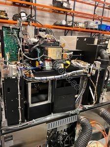
The AIT II is a patterned wafer inspection system for 150 to 300 mm wafers that provides fast, accurate feedback on process tool performance. It offers an integrated solution for automated defect classification and analysis, quickly turning defect data into yield-enhancing information. It is designed for flexibility in films, etch, photo, and CMP applications and offers advantages such as reducing process excursions, increasing overall equipment effectiveness, improving yield stability/predictability, and augmenting line monitoring.文件
无文件

类似上架物品
查看全部


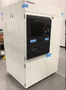


KLA
AIT II
类别
Defect Inspection
上次验证: 60 多天前


物品主要详细信息
状况:
Used
运行状况:
未知
产品编号:
125560
晶圆尺寸:
未知
年份:
未知
Logistics Support
Available
Transaction Insured by Moov
Available
Refurbishment Services
Available
说明
Wafer Test配置
无配置OEM 型号描述
The AIT II is a patterned wafer inspection system for 150 to 300 mm wafers that provides fast, accurate feedback on process tool performance. It offers an integrated solution for automated defect classification and analysis, quickly turning defect data into yield-enhancing information. It is designed for flexibility in films, etch, photo, and CMP applications and offers advantages such as reducing process excursions, increasing overall equipment effectiveness, improving yield stability/predictability, and augmenting line monitoring.文件
无文件