

说明
Particle Measurement配置
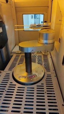
Process: BAREINSP Tool config is based on original PO, please verify tool details at tool inspection STANDARD SPECIFICATIONS Windows System Windows XP SP3 Main S/W NGS 5.4 SR3 HF3 Wafer Size 300mm SEMI Notch Carrier 3 AdvanTag SW CID, Phx, Shinko (load port) 8 user-configurable LEDs to display the loadport status Load/unload button for manual delivery hand-off Cassette / wafer mapping which allows the tool to generate a wafer map of the 300mm FOUP and detect wafer presence, empty slots and cross-slotted wafer. The wafer map can be displayed on the user screen and sent to a SECS host. Facilities Power: 208 VAC, 3W-N CDA: > 28.3 Nl/min, > 6.6791 kg/cm2 Vac: > 28.317 l/min, > -700 mm Hg Chamber Powder Coat Panels Kit 200/300mm Vacuum option Optical Filter Load port Vacuum 300mm Dual FIMS Application 2mm Edge Exclusion Oblique Incidence Illumination (High / Standard / Low) Normal Incidence Illumination (High / Standard / Low) Enhanced XY Coordinates IDM SP2 Standard Classification package LPD-N Classification LPD-ES classification Grading and Sorting Spatial Filter (20 degree) Spatial Filter (40 degree) Spatial filter (rough films) Spatial filter (Back) High Sensitivity Inspect Mode High Throughput Inspect Mode Options Haze Haze Normalization Haze Analysis IC/OEM Mfg Surf Quality Recipe Wafer size. 300mm XY Calibration Wafer with first Article HARDWARE CONFIGURATION Others 5 Color Light Tower (RBYGW) Ethernet NFS Client E84 enabled for OHT & AGV/RGV E87 (Based on E39) GEM/SECS and HSMS E40/ E94/ E90 / E116 Handler Secondary UI, Phoenix, SP2 Main Computer Intel®Xeon™ CPU 3.20GHz 3.5 GB RAM Memory DVD- ROM Mouse Keyboard 3.5" Floppy NGS application software FEC computer Intel®Pentium®4 CPU 512 MB RAM Memory Damage/Missing parts list Please inspect tool to reconfirmOEM 型号描述
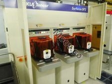
The Surfscan SP2 is an unpatterned wafer surface inspection tool that uses UV laser technology, darkfield optics, and advanced algorithms to detect defects as small as 30nm. It provides high sensitivity detection on engineered substrates and has a significant throughput increase over the prior-generation tool. It offers a single tool solution for three technology nodes and has comprehensive wafer surface inspection capabilities. It also enables faster root-cause analysis with improved coordinate accuracy and real-time defect classification capability.文件
无文件
KLA
SURFSCAN SP2

已验证
类别
Defect Inspection
物品主要详细信息
状况:
Used
运行状况:
未知
产品编号:
13216
晶圆尺寸:
12"/300mm
年份:
2010
Have Additional Questions?
Logistics Support
Available
Money Back Guarantee
Available
Transaction Insured by Moov
Available
Refurbishment Services
Available
类似上架物品
查看全部
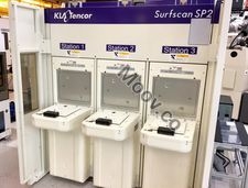
KLA
SURFSCAN SP2
已验证
类别
Defect Inspection
上次验证: 30 多天前


物品主要详细信息
状况:
Used
运行状况:
未知
产品编号:
13216
晶圆尺寸:
12"/300mm
年份:
2010
Logistics Support
Available
Money Back Guarantee
Available
Transaction Insured by Moov
Available
Refurbishment Services
Available
说明
Particle Measurement配置
Process: BAREINSP Tool config is based on original PO, please verify tool details at tool inspection STANDARD SPECIFICATIONS Windows System Windows XP SP3 Main S/W NGS 5.4 SR3 HF3 Wafer Size 300mm SEMI Notch Carrier 3 AdvanTag SW CID, Phx, Shinko (load port) 8 user-configurable LEDs to display the loadport status Load/unload button for manual delivery hand-off Cassette / wafer mapping which allows the tool to generate a wafer map of the 300mm FOUP and detect wafer presence, empty slots and cross-slotted wafer. The wafer map can be displayed on the user screen and sent to a SECS host. Facilities Power: 208 VAC, 3W-N CDA: > 28.3 Nl/min, > 6.6791 kg/cm2 Vac: > 28.317 l/min, > -700 mm Hg Chamber Powder Coat Panels Kit 200/300mm Vacuum option Optical Filter Load port Vacuum 300mm Dual FIMS Application 2mm Edge Exclusion Oblique Incidence Illumination (High / Standard / Low) Normal Incidence Illumination (High / Standard / Low) Enhanced XY Coordinates IDM SP2 Standard Classification package LPD-N Classification LPD-ES classification Grading and Sorting Spatial Filter (20 degree) Spatial Filter (40 degree) Spatial filter (rough films) Spatial filter (Back) High Sensitivity Inspect Mode High Throughput Inspect Mode Options Haze Haze Normalization Haze Analysis IC/OEM Mfg Surf Quality Recipe Wafer size. 300mm XY Calibration Wafer with first Article HARDWARE CONFIGURATION Others 5 Color Light Tower (RBYGW) Ethernet NFS Client E84 enabled for OHT & AGV/RGV E87 (Based on E39) GEM/SECS and HSMS E40/ E94/ E90 / E116 Handler Secondary UI, Phoenix, SP2 Main Computer Intel®Xeon™ CPU 3.20GHz 3.5 GB RAM Memory DVD- ROM Mouse Keyboard 3.5" Floppy NGS application software FEC computer Intel®Pentium®4 CPU 512 MB RAM Memory Damage/Missing parts list Please inspect tool to reconfirmOEM 型号描述
The Surfscan SP2 is an unpatterned wafer surface inspection tool that uses UV laser technology, darkfield optics, and advanced algorithms to detect defects as small as 30nm. It provides high sensitivity detection on engineered substrates and has a significant throughput increase over the prior-generation tool. It offers a single tool solution for three technology nodes and has comprehensive wafer surface inspection capabilities. It also enables faster root-cause analysis with improved coordinate accuracy and real-time defect classification capability.文件
无文件